


Researchers 'grow' lasers in chip breakthrough
The DARPA-funded work could cut costs and SWAP for microsystems used in radars, sensors and communications devices.
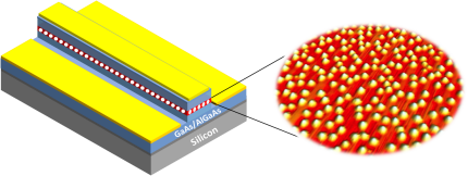
An optical micrograph by DARPA shows lasers integrated on silicon substrates.
Researchers from the University of California, Santa Barbara have reported a breakthrough in chip design that integrates electronic and photonic components and could lead to smaller, lighter, more power-efficient and less expensive microsystems of the kind used in radar, communications, imaging and sensing devices.
In work funded by the Defense Advanced Research Projects Agency, the researchers have managed to place billions of light-emitting dots, or “quantum dots,” directly onto silicon, a process that avoids more involved and expensive procedures, DARPA said in a release. The research was done as part of DARPA’s Electronic-Photonic Heterogeneous Integration (E-PHI) program.
“It is anticipated that these E-PHI demonstrator microsystems will provide considerable performance improvement and size reduction versus state-of-the-art technologies,” Josh Conway, E-PHI’s program manager, said. “Not only can lasers be easily integrated onto silicon, but other components can as well, paving the way for advanced photonic integrated circuits with far more functionality than can be achieved today.”
Microsystems devices generally need to be tailored to the application they’re to be used for, which precludes a uniform manufacturing process, DARPA said. Integrating the substrates and processing technologies to date has required combining microchips, which can limit bandwidth and introduce latency. The E-PHI program set out in 2011 to get around this problem by “integrating chip-scale photonic microsystems with high-speed electronics directly on a single silicon microchip,” DARPA said.
The UCSB researchers showed how they created the quantum dots by depositing, or “growing,” layers of indium arsenide material directly onto silicon wafers, integrating electronic and photonic circuits on a common surface. This process would eliminate the need for wafer bonding, a more expensive process for adding photonic components to silicon.
The results will reduce the size, weight and power requirements for those microsystems, as well as their assembly and packaging costs, DARPA said.